Manufacturing Methods for AlInN Films and Two-Dimensional Photonic Crystal Resonators
January 4, 2021
An AlInN film formed on a GaN film with a surface flatness of 3mm or lower
Key Word : photonic crystal resonator, hollow structure, sacrificial layer, GaN, MEMS
Background / Context / Abstract:
In fabricating a light-emitting device using a two-dimensional photonic crystal resonator (not limited to this but including a wide range of semiconductor light-emitting devices), it is essential to fabricate a structure to float the light-emitting layer in hollowness in order to improve the light-emitting efficiency. To fabricate the hollow structure, a sacrificial layer is required in the lower part of the light-emitting layer. The sacrificial layer in which selective wet etching is possible and which can grow into sufficiently thick film is required. Recently, GaN (gallium nitride)-based light-emitting devices have been developed, and for a sacrificial layer material compatible with this GaN (=material whose lattice constant is similar to that of GaN, which can be lattice-matched to GaN, and with which a high-efficiency light-emitting device is able to be fabricated), AlInN (aluminum indium nitride) is available.
In particular, Al0.82In0.18N which contains 18% In is known to be lattice-matched with GaN, and its importance as the sacrificial layer attracts attention: however, its thick-film growth (for example, 300 nm or more) has not yet been achieved. In general, when the AlInN film thickness becomes 100 nm or more, the surface condition is degraded and surface irregularities increase, and the crystal quality deteriorates. The reason why surface irregularities increase is that In deposits on the surface as droplets. Consequently, the development of techniques for fabricating a high-quality AlInN film whose surface is flat on the atomic layer level is strongly required.
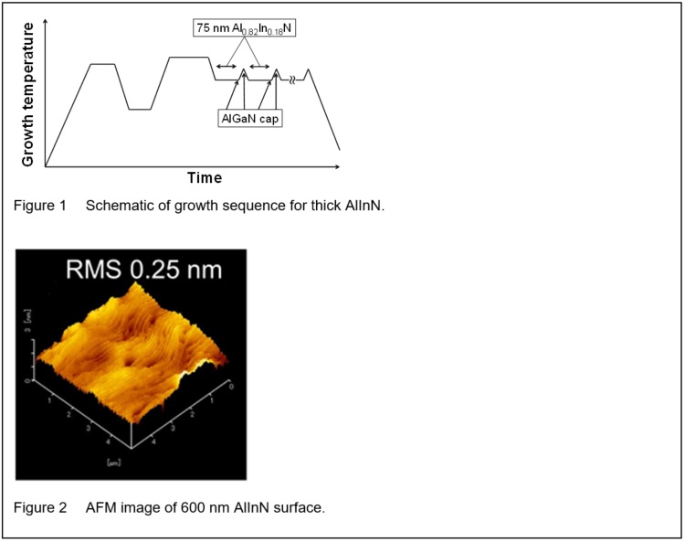
The inventors have accomplished the present invention by allowing a GaN cap layer to grow on the AlInN film when the AlInN film used for the sacrificial film is fabricated, in which high quality (small surface irregularities) and thick film growth (600 nm) of AlInN are achieved by evaporating to remove the In droplets on the surface by the use of a technique repeating “Step [1] The AlInN layer grows at a predetermined temperature Step [2] The AlGaN (or GaN) cap layer grows at the same temperature as in Step [1] Step [3] The temperature is raised from Step [2] to allow the AlGaN (or GaN) cap layer to further grow Step [4] The temperature is lowered, and the operation is returned to Step [1]).
Technology Overview:
An AlInN film formed on a GaN film, whose root-mean-square height RMS that indicates the surface flatness is 3 nm or lower, and for which the AlInN and the cap layer above it are manufactured by a method of repeating the temperature raising and temperature lowering sequence. Also a two-dimensional photonic crystal resonator using the AlInN film.
Benefits:
With an additive-free GaN layer grown on a sapphire substrate, a sequence of [1] growing an AlInN layer by 75 nm at 800°C, [2] continuously growing an AlGaN cap layer by 3 nm at 800°C, [3] growing the AlGaN cap layer further by 3 nm at 1,000°C, and [4] the temperature is lowered to 800°C and the step returns to [1] was repeated 8 times. As a result, an AlInN layer whose root-mean-square height RMS that indicates the surface flatness was 0.17 nm, which contains 18% In, and which is 600 nm thick (= 75 nm x 8 times) was successfully fabricated for the first time in the world.
Potential Applications / Potential Markets:
・A two-dimensional photonic crystal resonator (low-threshold laser diode)
・AlInN film as an intermediate material of the resonator
・GaN-based MEMS
State of Development / Opportunity / Seeking:
●Opportunity
・Available for exclusive and non-exclusive licensing
・Exclusive/non-exclusive evaluation for defined period (set up for options)
・Collaborative/supportive research
●Seeking
・Licensing
・Development partner
IP Status:
WO2018/159531 (PCT applied in Japanese), Applied in Taiwan
Figures:
Contact:
![]()