Dual-mode, high-sensitivity, near-infrared, polymer optical sensor base on the thicker active layer
May 19, 2022
Background / Context / Abstract:
Printed organic photoelectric conversion devices have attracted considerable attention in recent years due to their advantages, such as potential flexibility, large-area detection, and so forth over their inorganic counterparts. In general, narrowband applications such as industrial colorimetric measurements, spectral biological imaging, etc., typically use broadband photodetectors combined with additional color filters.
The bulk heterojunction (BHJ) devices with large donor (D)/acceptor (A) interface areas exhibit relatively high IPCE. Many conjugated polymers have the high absorption coefficient in the order of 105 cm-1. In a conventional organic solar cell (light-receiving) element, a thin organic film of approximately 0.1 μm is thick enough to absorb an adequate amount of light and exhibit typical photovoltaic characteristics. In general, phase-separated-type BHJ is suitable for organic solar cells. On the other hand, we propose that interpenetrating network-type BHJ is ideal for the NIR device. Thus, in this technology, high responsive polymer NIR devices have been developing by utilizing the weak sub-bandgap absorption owing to the interface between D/A materials. The present invention can detect a near-infrared narrow band with an external quantum efficiency exceeding 100% without a color filter by utilizing weak absorption owing to charge transfer between D and A molecules by designing an element with an active layer film thickness several ten times or more than that of a conventional one. (Figure 1). (Figure 2, 3) It also has the feature of functioning as a typical photodiode under reverse bias. For a device with an intermediate film thickness, it also has the potential for use as a self-powered device and sensitivity in the near-infrared region. (Figure 4)
[Expectation]
- With the aim of commercializing a near-infrared sensor using this technology, we hope to collaborate with companies developing optical sensors with printed-device fabrication technology.
- We hope to engage in joint research with companies developing organic functional materials with absorption in the near-infrared region.
[Researcher]
Division of Electrical, Electronic and Infocommunications Engineering, Graduate School of Engineering, Osaka University
Associate Professor Hirotake Kajii
Benefits:
Advantages
Organic near-infrared (NIR) photoelectric conversion devices based on thicker bulk heterojunction films
- High detection sensitivity in the near-infrared region with an external quantum efficiency (IPCE) exceeding 100% under forward bias
- Functions as a typical photodiode under reverse bias
- Narrow bandwidth detection without color filters
- Potential flexibility, large-area detection, printed fabrication process
Although functioning as a typical solar cell, it can also serve as a self-powered device with the function of a detection sensor with sensitivity in the near-infrared region by intermittently applying a forward bias equal to or higher than the open-circuit voltage, Voc.
Potential Applications / Potential Markets:
Near-infrared sensors
State of Development / Opportunity / Seeking:
・Available for exclusive and non-exclusive licensing
・Exclusive/non-exclusive evaluation for defined period (set up for options)
・Collaborative/supportive research
※Seeking
1. Development partner
2. Licensing
IP Status:
Applied in Japan (JPO), not yet published.
Figures:
[Data, etc.]
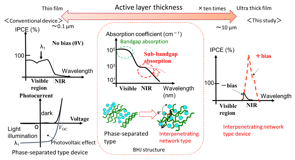
Figure 1 Comparison of the proposed device and the conventional device
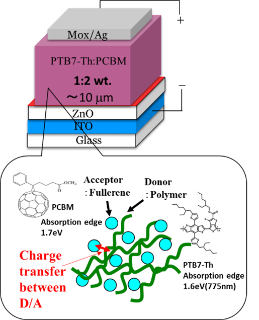
Figure 2 Inverted device structure with an ultra-thick active layer for near-infrared narrowband detection
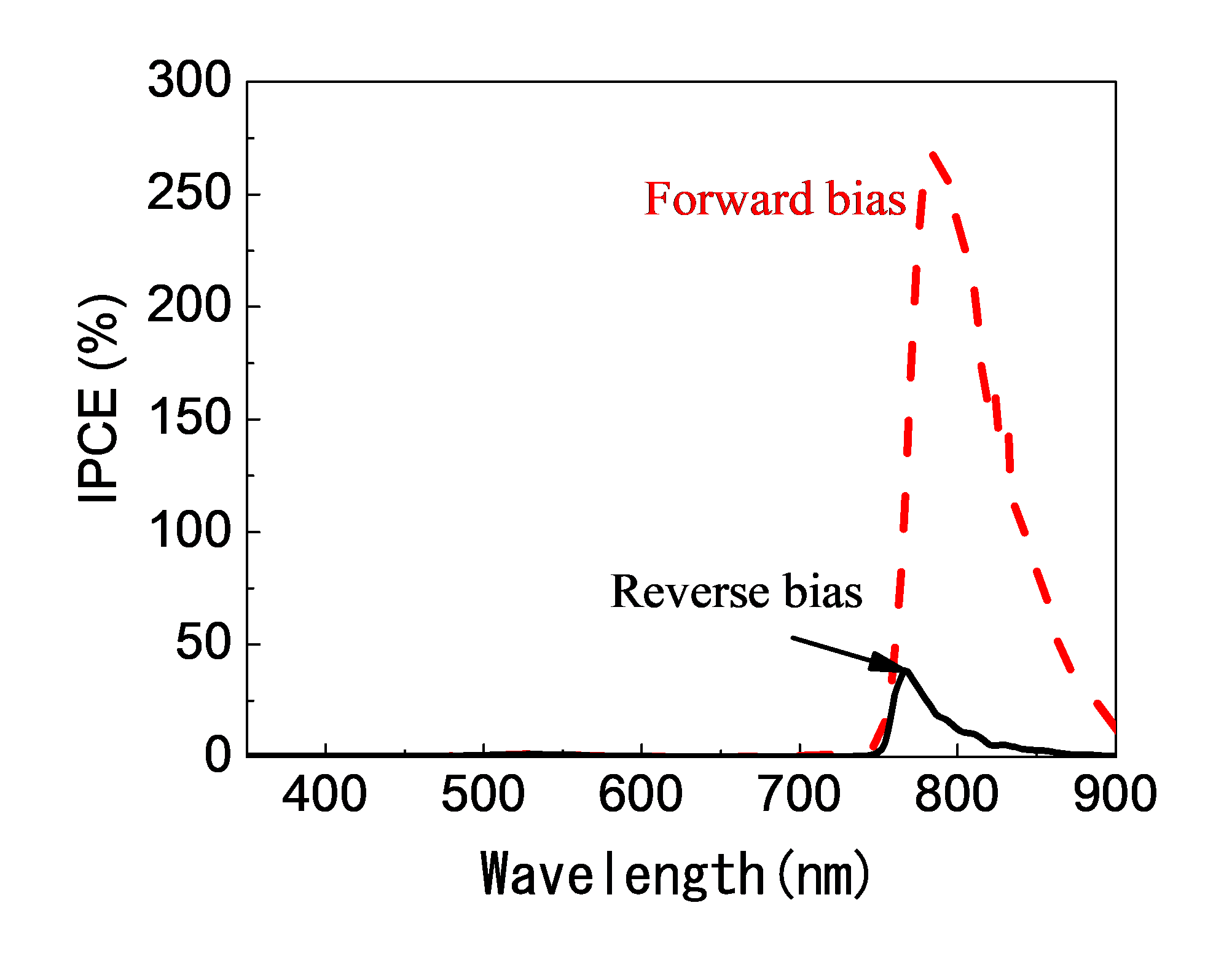
Figure 3 IPCE characteristics of a device with an ultra-thick active layer under forward and reverse biases
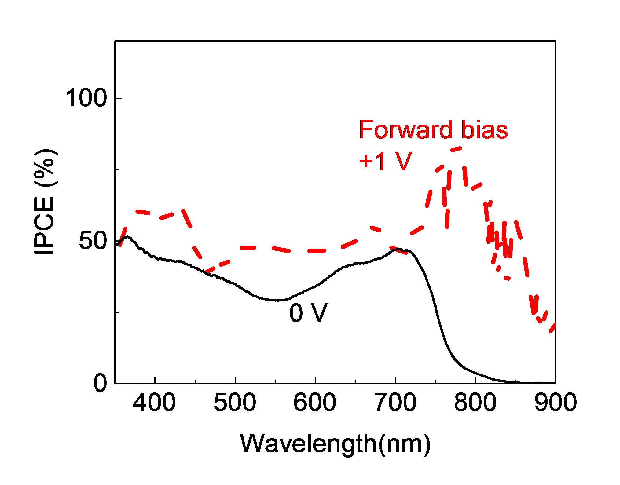
Figure 4 IPCE characteristics of a device with an intermediate film thickness under no bias and forward bias
Contact:
![]()